
China's Leading Clock IC Supplier
Precision Timing, Robust Reliability
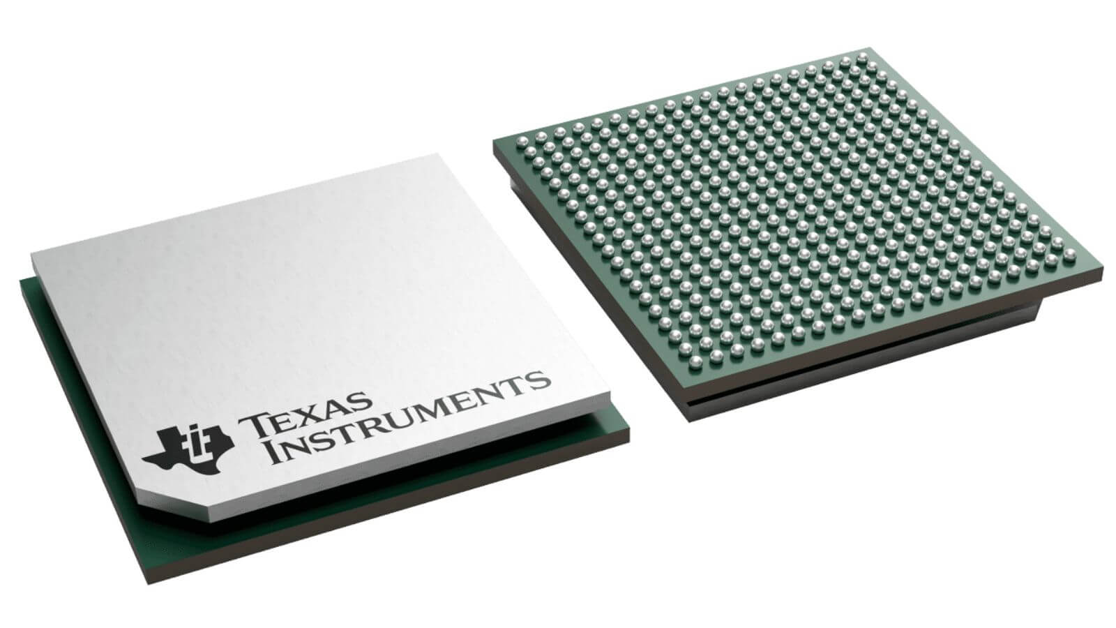
High-Precision Clock Integrated Circuits


What Are Clock, Timing & Data Converter ICs?
Clock, timing, and data converter integrated circuits form the temporal and amplitude backbone of modern digital systems, orchestrating signal synchronization, frequency generation, and analog-digital domain translation. These devices enable precise time-base generation for microprocessors and communication interfaces, manage clock distribution across multi-chip architectures, and convert continuous analog signals into discrete digital representations (and vice versa) with resolution ranging from 8 to 32 bits and sampling rates from kHz to GHz.
Core Functions
- Clock Generation & Synthesis: Creating stable, low-jitter clock signals from reference oscillators using PLLs (Phase-Locked Loops) and VCOs (Voltage-Controlled Oscillators), enabling frequency multiplication (×N), division (÷M), and programmable output frequencies from kHz to GHz for system synchronization, CPU/GPU clocking, and communication timing (±10ppm to ±50ppm stability, <1ps RMS jitter for high-speed interfaces).
- Clock Distribution & Buffering: Fanout and routing of clock signals to multiple system components with controlled skew (<50ps), low additive jitter (<0.5ps), and programmable output formats (LVDS, LVPECL, HCSL, CMOS) to maintain timing integrity across PCBs in servers, networking equipment, and test instrumentation where synchronous operation of 10–100+ devices is critical.
- Analog-to-Digital Conversion (ADC): Sampling continuous analog signals (voltage, current, sensor outputs) and quantizing them into digital words with resolution from 8-bit (±0.4% error) to 24-bit (±0.0001% error) at sampling rates from 100kSPS to 10GSPS, employing architectures including SAR (successive approximation), delta-sigma (Σ-Δ), pipeline, and flash ADCs optimized for different speed-accuracy-power trade-offs.
- Digital-to-Analog Conversion (DAC): Reconstructing analog signals from digital codes for waveform generation, control loops, and communication modulation with resolution from 8-bit to 20-bit, settling times from ns to µs, and output types including voltage (0–10V, ±10V), current (4–20mA), and differential current (for RF applications), maintaining linearity (INL/DNL <±0.5 LSB) and low glitch energy for smooth signal reconstruction.
Technical Principles
Clock synthesizers employ charge-pump PLLs with integrated VCOs and loop filters to lock output frequency to a stable crystal reference (10MHz–100MHz TCXO/OCXO). The PLL compares the phase of a divided output signal against the reference using a phase-frequency detector (PFD), generating error correction through a charge pump that adjusts VCO control voltage until phase alignment is achieved. Modern jitter cleaners use fractional-N synthesis and clock recovery circuits to regenerate clean clocks from jittered inputs (up to 100ps p-p input jitter reduced to <1ps RMS output jitter), essential for recovering data from SerDes links and cleaning up signals in clock distribution trees.
SAR ADCs dominate precision measurement applications (12–18 bit, 100kSPS–10MSPS), using a binary search algorithm and switched-capacitor DAC to converge on the input voltage in N clock cycles. Delta-sigma ADCs achieve highest resolution (16–32 bit) at moderate speeds (10SPS–1MSPS) through oversampling and noise-shaping, integrating quantization noise out-of-band for near-ideal signal-to-noise ratio (SNR >120dB) in audio, industrial sensors, and weighing scales. Pipeline and flash ADCs sacrifice power for speed (8–14 bit, 10MSPS–5GSPS), parallelizing conversion stages for high-throughput applications like software-defined radio (SDR), oscilloscopes, and radar signal processing.
DACs employ resistor ladder (R-2R), current steering, or delta-sigma modulation architectures. Current-steering DACs achieve fastest settling (<10ns) and highest update rates (>1GSPS) for arbitrary waveform generators and RF signal synthesis, using matched current sources switched by a thermometer or segmented decoder. String DACs (resistor ladder) provide excellent monotonicity and low glitch energy for control applications (motor speed, power supply trim), while delta-sigma DACs offer best linearity (THD+N <-100dB) for audio reproduction and precision voltage references despite slower response times.
Data Converter Integrated Circuits
Unit Electronics specializes in high-performance Data Converter Integrated Circuits, catering to industrial, automotive, and communications systems worldwide. Our extensive product line includes analog-to-digital converters (ADCs), digital potentiometers (digipots), digital-to-analog converters (DACs), and integrated & special-function data converters. Engineered for efficiency and reliability, our solutions simplify system design, enhance accuracy, expand bandwidth, and minimize power consumption and solution size—all supported by our evaluation modules and application notes. With a focus on innovation, we deliver tailored data converter technologies that meet diverse project needs, ensuring seamless integration and optimal performance for every application.
Data Converter ICs Types
Analog-to-digital converters (ADCs)
Digital potentiometers (digipots)
Digital-to-analog converters (DACs)
Integrated & special-function data converters
High-Performance Clock, Timing & Data Converter Solutions
Since 2016, Unit Electronics Co., Ltd. has been delivering premium clock generators, timing controllers, ADCs, and DACs with full documentation, original quality, and fast global delivery for manufacturers and distributors worldwide.
Precision Timing & Data Conversion in Critical Systems
Exploring how ultra-low jitter clock generators, high-resolution ADCs, and precision DACs enable synchronous data processing, accurate signal acquisition, and waveform generation in telecommunications, test equipment, industrial control, and medical imaging systems.

Telecommunications
5G Base Station Timing
High-Speed Data Conversion

Test & Measurement
Oscilloscopes & Spectrum Analyzers
Arbitrary Waveform Generators

Industrial Automation
Precision Sensor Measurement
Motor Control & Drives

Medical Imaging
Ultrasound Beamforming
CT & X-Ray Detectors

Data Centers & Servers
Multi-Core CPU Clocking
Power Management Telemetry
Automotive Electronics
ADAS Sensor Processing
Battery & Powertrain Monitoring
Frequently Asked Questions
Find answers to common questions about our Clock, Timing & Data Converter IC products and services.
What types of ADCs and DACs do you supply?
We supply SAR ADCs (8–18 bit, 10kSPS–20MSPS), delta-sigma ADCs (16–32 bit, 10SPS–10MSPS), pipeline ADCs (10–16 bit, 10MSPS–500MSPS), flash/interleaved ADCs (8–14 bit, 100MSPS–10GSPS), and specialized ADCs (isolated, automotive, audio). DAC offerings include R-2R DACs (8–16 bit), current-steering DACs (10–16 bit, up to 10GSPS), string DACs, delta-sigma DACs (audio, 24-bit), and digital potentiometers (6–10 bit, I2C/SPI) from TI, ADI, Microchip, Maxim, and Linear Technology.
How do I choose between SAR, delta-sigma, and pipeline ADCs?
SAR ADCs: Best for precision measurement (12–18 bit) at moderate speeds (10kSPS–10MSPS) with low power. Delta-sigma ADCs: Highest resolution (16–32 bit), best SNR (>120dB), but slower (10SPS–1MSPS)—ideal for audio, weighing scales, industrial sensors. Pipeline ADCs: Balanced speed (10–16 bit, 10MSPS–500MSPS) and resolution for imaging, communications, software-defined radio. Flash ADCs: Fastest (GSPS range) but lower resolution (8–12 bit), highest power—oscilloscopes, radar, high-speed test equipment.
What are the key differences between TCXO, OCXO, and VCXO clock oscillators?
TCXO uses temperature compensation circuits for ±0.5–2ppm stability with low power consumption, suitable for portable devices. OCXO uses an oven-controlled cavity for ±0.01–0.1ppm ultra-high stability, ideal for telecom and test equipment. VCXO allows voltage-controlled frequency tuning (±50–200ppm), used in PLL and clock recovery circuits where frequency adjustment is needed.
How do your clock and timing ICs meet automotive-grade AEC-Q100 reliability requirements?
Our automotive-grade clock ICs are AEC-Q100 qualified, supporting an operating temperature range of -40°C to +125°C, with enhanced ESD protection and PPAP documentation available. They are designed for vehicle applications including T-BOX, ADAS, and in-vehicle infotainment systems.
How do your timing solutions support 5G base station synchronization (IEEE 1588/SyncE)?
We supply IEEE 1588 PTP-compliant and SyncE-capable clock ICs with sub-100fs jitter performance and DPLL functionality, enabling frequency and phase synchronization for 5G fronthaul and backhaul equipment in compliance with ITU-T G.8262/G.8273 standards.
What is your minimum order quantity (MOQ) and typical lead time for clock and data converter ICs?
MOQ is typically 1 piece for in-stock items, with no minimum for sample requests. Standard lead time is 3–7 business days for stocked parts; 4–12 weeks for non-stocked or special-order components. Contact sales@unitsemi.com for real-time inventory and delivery confirmation.
Do you provide evaluation boards and reference designs?
Yes, we link to manufacturer evaluation modules (EVMs) with schematics, PCB layouts (high-speed layout guidelines for ADCs/DACs), BOM, and software drivers (LabVIEW, MATLAB, Python, C code). Reference designs include multi-channel data acquisition systems (simultaneous sampling, multiplexed inputs), precision analog front-ends (AFE), clock distribution networks for JESD204B/C ADC/DAC interfaces, and clock jitter measurement setups. Application notes cover anti-aliasing filter design, grounding/decoupling best practices, and ENOB optimization techniques.
Ready to Optimize Your Signal Chain?
Contact our timing and data conversion engineering team today to receive detailed quotations tailored to your precision requirements. Fast response within 24 hours with technical recommendations for optimal component selection.
